Technologies and ApplicationsAtomic Layer Deposition (ALD)
ALD achieves precise film thickness control at the atomic layer level, producing smooth, dense thin films. The technique enables conformal deposition on substrates ranging from planar surfaces such as Si wafers to high-aspect-ratio 3D structures. This page covers the fundamental principles and key concepts behind ALD, along with the film characteristics produced—including conformality.
Film Formation Principle: Self-Limiting
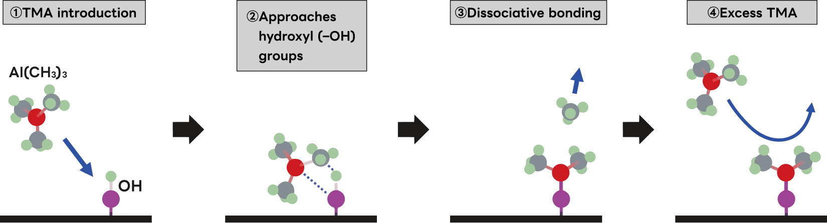
Self-limiting reaction is the defining mechanism of ALD. The following explains this principle using trimethylaluminum (TMA: Al(CH₃)₃) as an example.
- ①When the introduced TMA approaches a hydroxyl group (OH),
- ②the bond between the Al atom(●in the figure)of the TMA and the C atom(●in the figure)of the methyl (CH₃) group weakens, and the CH₃ group attempts to bond with the H atom (●in the figure)of the OH group, while the Al atom attempts to bond with the O atom(●in the figure)of the OH group.
- ③As they approach further, the CH₃ group bonds with the H atom to form methane (CH₄) and detaches from the substrate, while the Al atom forms a covalent bond with the O atom and adheres to the substrate.
- ④If the substrate surface is filled with the Al(CH3)2 layer formed in process ③, the next TMA that arrives cannot react and is vented.
Because no OH groups remain available as reaction partners, subsequent TMA molecules cannot contribute to film growth and are purged. This phenomenon - where the completion of a single atomic or molecular layer terminates further reaction with the next precursor - is called self-limiting.
Film Formation Process: Pulse (Digital) Growth
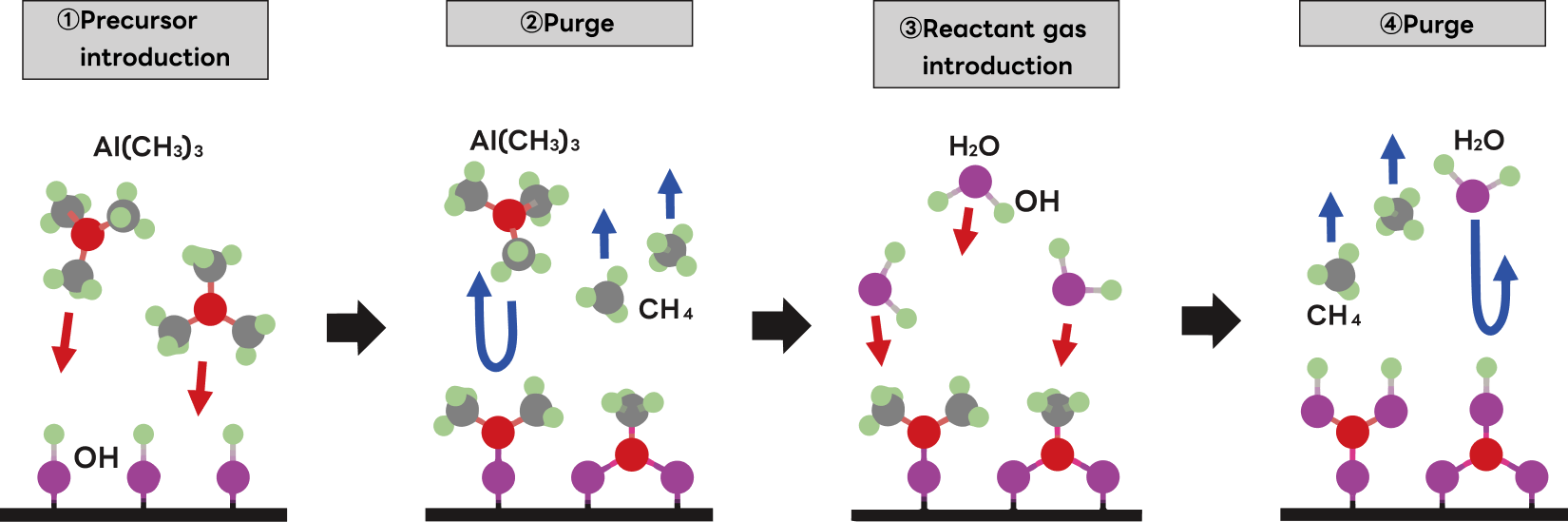
What sets ALD apart from other thin-film deposition methods is that each cycle deposits exactly one atomic or molecular layer through a four-step pulse sequence; film thickness grows by repeating this cycle. For this reason, ALD is also referred to as pulse deposition, digital deposition, or layer-by-layer deposition. The following describes this process using aluminum oxide (Al₂O₃) film growth as an example, with trimethylaluminum (TMA: Al(CH₃)₃) as the precursor and water as the reactant.
- ①Precursor Introduction
Si wafer surfaces naturally bear hydroxyl groups (OH) formed by reaction with atmospheric moisture. As TMA is introduced and approaches the wafer surface, the methyl group (CH₃) of TMA abstracts a hydrogen atom from an OH group, forming methane (CH₄) which departs from the surface. Simultaneously, the Al atom forms a new covalent Al–O bond with the oxygen remaining on the wafer. - ②Purge
An inert carrier gas (N₂ or Ar) is flowed to purge excess TMA and CH₄ byproduct that did not contribute to film growth. - ③Reaction Gas Introduction
Once excess TMA and CH₄ byproduct have been fully removed, water is introduced. Each H₂O molecule approaching a surface-bound CH₃ group dissociates into H and OH: the H combines with CH₃ to form CH₄ (which departs), while the OH bonds to the Al atom, terminating the surface as Al–OH. Once all available Al sites are saturated, additional water molecules find no reaction partners and are purged—as in step ①, self-limiting behavior again governs the process. - ④Purge
An inert carrier gas (N₂ or Ar) is flowed to purge excess H₂O and CH₄ byproduct from the previous step.
Completion of steps ① through ④ deposits one Al–O monolayer, leaving the surface terminated with OH groups. Repeating this four-step cycle builds up a thin Al₂O₃ film with atomic-layer-level thickness control.
Characteristics of ALD
The ALD process and the films it produces offer the following key characteristics:
-
・Uniform deposition—in both thickness and film quality—is achievable on complex 3D structures and nanoscale surfaces, including high-aspect-ratio trenches, voids, and steps.
As shown in the comparison figure, sputtering suffers from directional shadowing that makes coverage of narrow features difficult, and while plasma CVD can follow complex geometries, conformally coating the inner walls of high-aspect-ratio pores remains challenging. - ・Films are highly dense, near-stoichiometric in composition, and pinhole-free.
- ・Covalent bonding with the substrate results in excellent adhesion to both the substrate and underlying material.
- ・The cycle-based process is highly reproducible, enabling precise, strict control of film thickness.
- ・Deposition is possible at lower substrate temperatures than most competing methods.

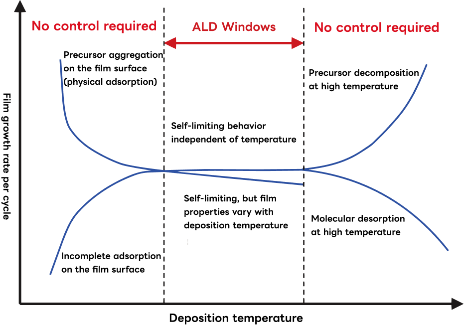
ALD Window
The self-limiting behavior that defines ALD depends on careful optimization of process parameters—including gas flow rate, pulse duration, pressure, and temperature. The range of conditions within which ideal self-limiting growth is maintained is known as the ALD Window.
- ・Below the ALD window, precursors reaching the substrate can form intermolecular bonds with subsequently arriving molecules, causing uncontrolled condensation-type film growth. Since this aggregation reaction is promoted at lower temperatures, film thickness tends to increase as temperature decreases. Conversely, the desired surface chemical reactions also slow at lower temperatures, reducing the growth rate of the target compound film.
- ・Above the ALD window, precursor molecules may decompose thermally, driving uncontrolled continuous film growth. Alternatively, adsorbed precursors may desorb and be evacuated before they can react.
- ・Even within the ALD window, an amorphous-to-crystalline phase transition may occur as temperature increases, raising film density and in some cases reducing the apparent growth rate per cycle.
The ALD window varies with process conditions including the choice of precursor, reactant gas, plasma source, substrate temperature, and vacuum system pumping performance.
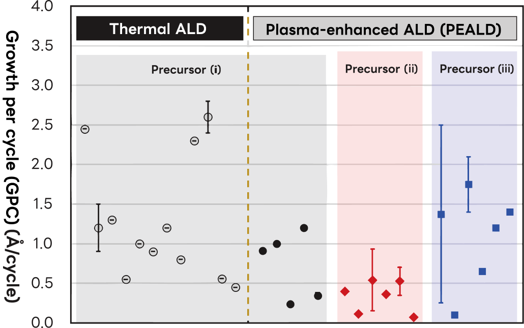
Differences in Film Quality and Growth Depending on Precursor and Reagent Types
Using SiNx films as an example, we outline how film growth per cycle varies with precursor and reactant type. Precursors are broadly classified into three groups:
- (ⅰ)those containing chlorine (e.g., SiH₂Cl₂, Si₂Cl₆),
- (ⅱ)carbon-containing precursors (e.g., 3DMAS: SiH(N(CH3)2)3, BTBAS: SiH2(NHtBu)2),
- (ⅲ)those containing neither chlorine nor carbon (SiH4, TSA: (N(SiH3)3, NPS: (SiH3)4Si, etc.)
Each group is further subdivided by process type: thermal ALD or plasma ALD.
The film properties obtained for each group are summarized below.
- ・Precursor (i) is widely used owing to its low cost and good stability, with an extensive body of research to draw from. However, chlorine incorporation as an impurity in the deposited film is a known concern.
- ・Precursor (ii) eliminates chlorine contamination, though carbon is introduced into the film. Under optimized conditions, however, carbon content can be limited to approximately 2 at.%, enabling the deposition of high-density, high-refractive-index SiNx.
- ・Precursor (iii) introduces no risk of Cl or C contamination. TSA and NPS offer a high Si content per molecule, suggesting favorable growth rates. TSA-based processes have yielded high-density, high-refractive-index SiNx films; NPS enables deposition at lower temperatures, albeit with slightly reduced density and refractive index.
Significant variations in film growth and quality observed even within the same precursor group are attributable to differences in substrate temperature, reactant gas type, and plasma source. Achieving target film quality therefore requires systematic optimization of a broad set of process parameters: precursor selection, reactant gas type, heat or plasma source, substrate temperature, precursor pulse and purge timing, and vacuum system performance.
(Reference) X. Meng et al., Materials 9, 1007 (2016).
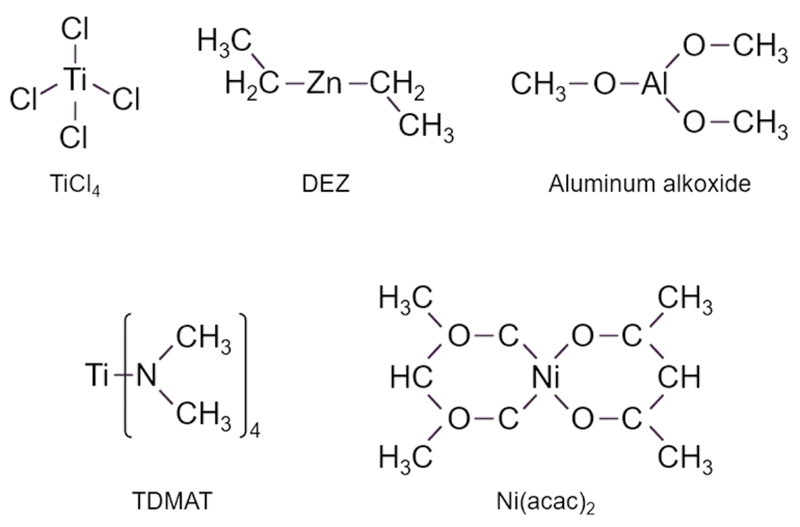
Precursors
As discussed in the ALD Window section, maintaining self-limiting behavior imposes strict constraints on allowable process conditions, making precursor selection and handling critically important. A wide variety of precursors tailored to specific deposition processes are commercially available from materials suppliers worldwide. The table below lists representative examples of ALD precursors currently in use or under active research.
| Compound | Chemical |
|---|---|
| Halogen | WF₆ |
| TiCl₄ | |
| HfCl₄ | |
| SnCl₄ | |
| Alkyl | Al(CH₃)₃: TMA |
| Zn(C₂H₅)₂: DEZ | |
| Alkoxide | Al(OCH₃)₃ |
| Ta(OC₂H₅)₅ | |
| Ti(OCH(CH₃)₃)₄ | |
| Alkylamide | Ti(N(CH₃)₂)₄: TDMAT |
| Zr(N(CH₃)(CH₂CH₃))₄: TEMAZ | |
| Ta(N(CH₃)₂)₅ | |
| Diketone | Cu(C₅HF₆O₂)₂: Cu(hfac)₂ |
| Ni(C₅H₇O₂)₂: Ni(acac)₂ | |
| Zr(C₁₁H₁₉O₂)₄: Zr(tmhd)₄ |
Plasma sources
Plasma-assisted deposition methods—such as sputtering and PECVD—leverage the high energy of plasma to synthesize compounds not readily formed thermally or to impart superior functional properties to the deposited film.
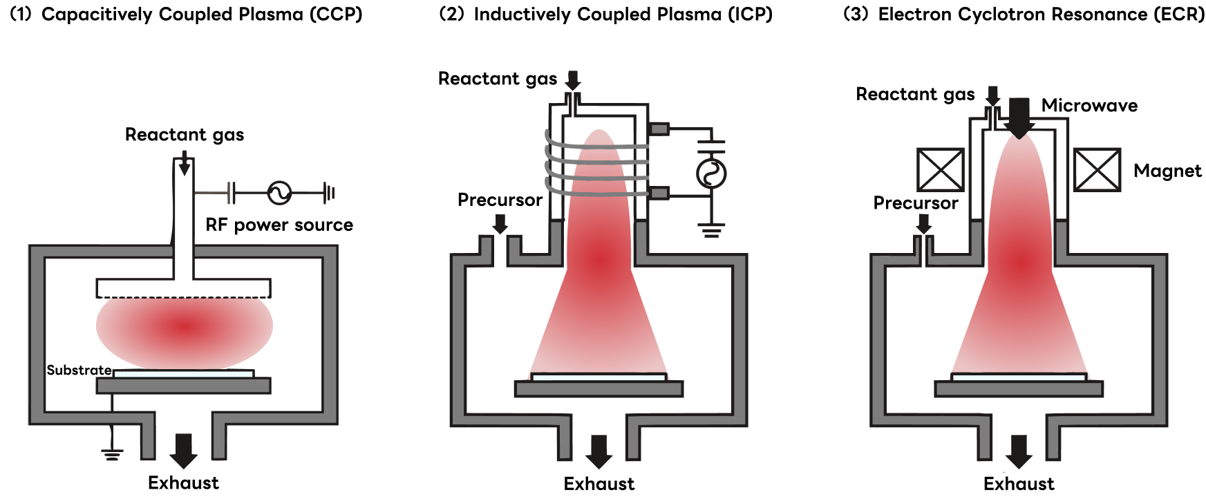
Three plasma source types are in widespread use:
- (1)Capacitively Coupled Plasma (CCP)
One electrode is connected to a high-frequency power source and the other is grounded. The oscillating electric field between them accelerates free electrons, which collide with and ionize surrounding atoms and molecules. The resulting ionized gas is capacitively coupled plasma. - (2)Inductively Coupled Plasma (ICP)
A high-frequency current through a coil generates a time-varying magnetic field that penetrates the vacuum chamber through a dielectric window. Electrons in the chamber circulate in closed paths (eddy currents) to oppose the changing flux, and are accelerated in the process. These energetic electrons collide with gas-phase atoms and molecules, causing ionization. The resulting ionized gas is inductively coupled plasma. - (3)Electron Cyclotron Resonance Plasma (ECR plasma)
Charged particles in a magnetic field gyrate around field lines; electrons, being far lighter than ions, rotate at much higher frequencies. When electromagnetic radiation at the electron cyclotron frequency is applied, electrons undergo resonant acceleration and gain sufficient energy to ionize surrounding gas molecules. In practice, 2.45 GHz microwaves are used, requiring a resonant magnetic field of 875 G.
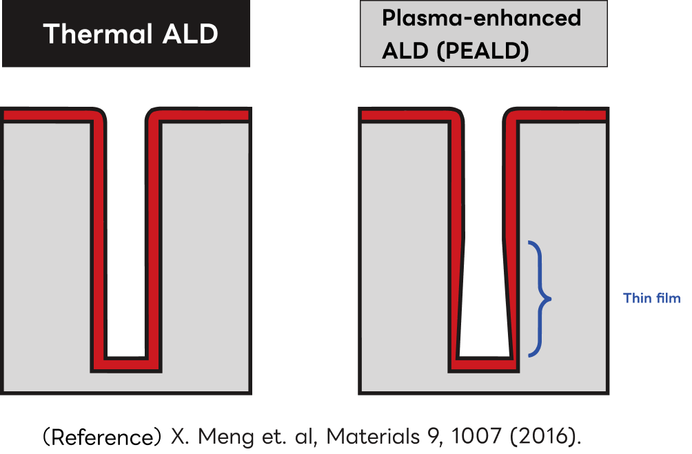
Differences in Film Quality and Thickness Uniformity Depending on the Reaction Source
Plasma ALD exploits the high chemical reactivity of electrons, ions, and radicals for thin-film formation. However, this same reactivity makes reactive species susceptible to deactivation: energy can be lost through collisions with surrounding atoms, molecules, or chamber walls, and ions can be neutralized by electron capture. In high-pressure environments or confined geometries—such as the interior of narrow trenches—reactive species deactivate before reaching the bottom, resulting in thinner films near the trench base (as shown in the figure). Extending plasma exposure time can compensate for this, but achieving uniform coverage at high aspect ratios remains extremely challenging depending on the AR and specific reaction chemistry. The plasma exposure time is managed accordingly.
Although plasma ALD offers significant advantages—including higher deposition rates and compatibility with lower substrate temperatures—it is inherently less capable than thermal ALD of achieving sidewall conformality in high-aspect-ratio trench structures.
Summary
ALD is an advanced thin-film deposition technique that leverages self-limiting surface reactions to achieve atomic-layer-level thickness control through the sequential repetition of four process steps. Historically, ALD was considered impractical for high-volume manufacturing due to the inherently slow, step-by-step nature of the process. The introduction of plasma enhancement has substantially increased deposition rates, and the development of large-scale batch equipment capable of processing multiple wafers simultaneously has transformed ALD into an indispensable technology for thin-film fabrication in nanotechnology applications—including semiconductor devices and MEMS/NEMS.