Technologies and ApplicationsDry Etching
The Principle of Dry Etching
Etching is a microfabrication process used to create desired circuit patterns on a wafer.
As it is generally performed after a resist mask has been formed, it is closely paired with lithography in the process flow, constituting the latter half of the patterning sequence.
The etching process enables microfabrication (at the micrometer-to-nanometer scale) and is an indispensable step in the fabrication of various devices, including semiconductors, flat-panel displays, MEMS, and optical devices.
Etching processes are broadly divided into two main categories:
- ➢Wet etching: performed in a chemical solution
- ➢Dry etching: performed in a discharge plasma or reactive gas environment within a vacuum chamber
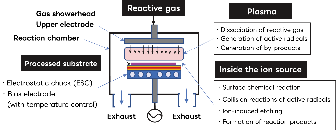
The following describes the typical configuration of a dry etching system and the phenomena related to the etching mechanism within the system.
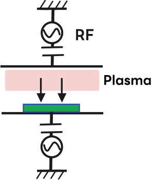
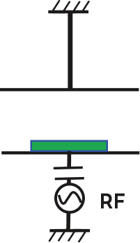
Inside the chamber, a pair of parallel plate electrodes is installed. A wafer is placed on the surface of one electrode, to which an RF voltage is applied, while the other electrode is maintained at ground potential and supplied with reactive gas through a showerhead mounted on its surface.
Plasma is generated between the electrodes by discharge, and gas molecules are excited to become reactive species that perform the etching action.
Chemical reactions between the reactive species and the wafer surface produce volatile etch products that are detached from the surface.
An ion sheath forms between the plasma and the electrode, bombarding the wafer surface with positive ions. This promotes radical driven chemical reactions, enhances the desorption of reaction products, and causes sputter etching. The desorbed reaction products become gaseous and are exhausted from the vacuum chamber.
| Wet etching | Dry Etching | Notes | |
|---|---|---|---|
| Etching rate | Fast | Slow | |
| Etching Uniformity | Poor | Good | Wet etching makes it difficult to control etch uniformity across the substrate surface |
| Process reproducibility | Poor | Good | |
| Endpoint detection | Not possible | Possible (plasma luminescence, ion mass spectrometry, laser profilometer, etc.) | Enables detection of the etch endpoint and control of etch depth to specification (high reproducibility) |
| CD loss (mask pattern line width – post-etch pattern line width) | Large | Small | In wet etching, etching proceeds beneath the resist, resulting in significant CD loss |
| Selectivity ratio relative to the photoresist | High | Low | Dry etching causes the photoresist to recede due to plasma. |
| Control of etch profile | Poor | Good | Dry etching offers high control over etch profiles through the control of process pressure, gas types, and ions in the plasma |
| Multilayer film etching | Difficult | Possible | Etching conditions can be switched according to the film (batch etching of multilayer films) |
| Etching progress | Isotropic | ① Anisotropic (physical etching) or ② Isotropic (chemical etching), etc., can be controlled |
|
| Environmental impact | Wet etching equipment generates acidic and alkaline waste liquids → High environmental impact | No waste liquid is generated, resulting in a low environmental impact. Exhaust gases are removed via plasma decomposition or through gas treatment equipment |
Dry etching equipment offers advantages in terms of SDGs compliance |
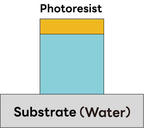
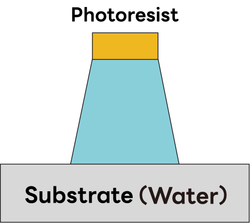
| Etching Profile | Side etching, Undercut 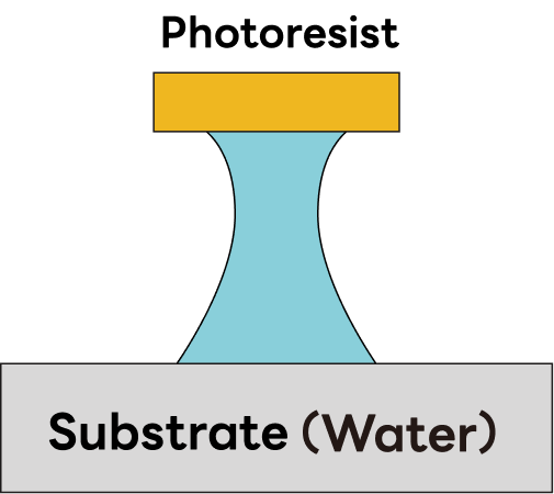
|
①Vertical profile
②Tapered profiles
|
Dry etching enables precise control of the etch profile across a range from vertical to tapered geometries. Profile shape is tuned by adjusting process parameters such as gas species, process pressure, RF power, and substrate temperature to meet the requirements of the target film. |
Etching Sources and Process Parameters
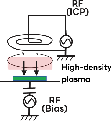
Although various plasma sources are used in dry etching, those utilizing ICP (inductively coupled plasma) are the most common.
ICP enables easy control of plasma distribution, generates high-density plasma at low pressure, and provides both improved etch rates and precise profile control.
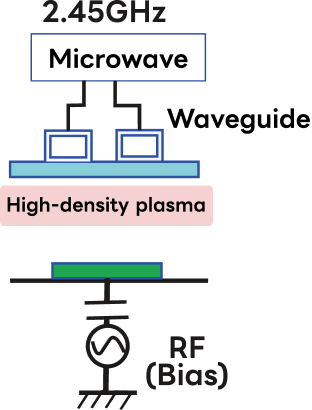
However, depending on the etching application, capacitive plasma (CCP), microwave plasma, and ion beam etching are also used as plasma sources.
| Etching Sources | Plasma Etching (PE Mode) |
Capacitive Plasma RIE (CCP-RIE) |
Inductively Coupled Plasma RIE (ICP-RIE) |
Microwave Plasma (MW Plasma Etch) |
Ion Beam Etch (IBE) |
|---|---|---|---|---|---|
| Plasma Densit [cm-3] | ~1E+10 | ~1E+10 | ~1E+12 | ~1E+12 | ~1E12 |
| Pressure range [mTorr] | 1000~100 | 500~10 | 100~1 | 1000~100 | ≦ 0.1 |
| Ion energy impinging on the substrate | Low | Medium | High | Medium | High |
| Reference Figure |
|
|
|
|
|
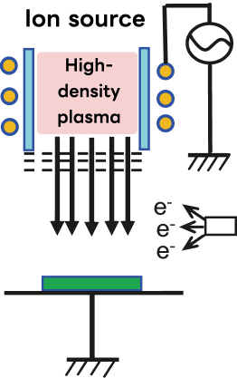
Mechanism of Ion Beam Etching
Ion beam etching (IBE) uses a focused beam of ions to remove material by physical sputtering, independently of chemical reactivity.
Because ion density and ion energy are controlled by separate parameters, IBE offers a unique combination of versatility and process control beyond the capability of plasma-based RIE systems.
Key characteristics of the IBE process are described below.
- ➢Ion density is controlled by the plasma source of the ion source, and ion energy is controlled by the DC acceleration voltage of the grid (negative bias voltage supplied by DC voltage). Therefore, each parameter can be controlled independently.
- ➢Since the process is performed at low pressures of ≤0.1 mTorr (roughly one order of magnitude lower than typical RIE systems), the mean free path of the ions is long, and energy loss due to collisions is minimal.
- ➢With a high acceleration voltage (>1 kV), etching rates of approximately 10–30 nm/min can be achieved.
- ➢It can be used on materials that cannot be etched by RIE (materials whose etching reaction products do not volatilize), and is used for etching materials such as copper (Cu), nickel (Ni), and gold (Au). Ion beam etching systems are also applied to the fabrication of oblique-angle diffraction gratings.
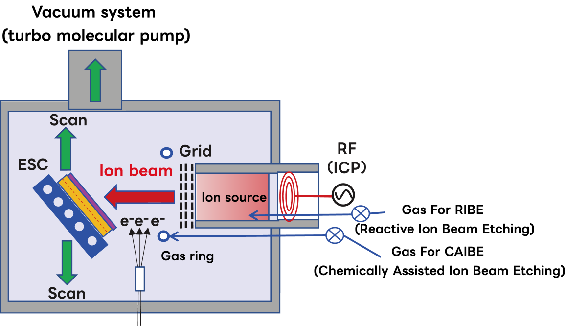
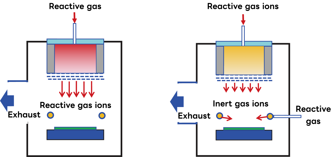
Classification of Ion Beam Etching Processes
・ RIBE (Reactive Ion Beam Etching):
Reactive gas is introduced into the plasma chamber of the ion source along with argon (Ar) gas; after ionization, it is accelerated through a grid and directed at the substrate as a reactive ion beam.
・ CAIBE (Chemical Assisted Ion Beam Etching):
Reactive gas is introduced into the reaction chamber downstream of the ion source, and etching is performed through the impact of Ar ions from the ion source and chemical reactions caused by the reactive gas.
Differences in the Reaction Processes for Each Etching Method
・Chemical Etching:
Free radicals (reactive species) react with the material being etched to perform the etching.
(Example) High-pressure reactive gas etching
・Physical etching and sputter etching:
Ions are accelerated by the local electric field (such as self-bias) and collide with the material being etched, performing physical etching.
・Ion-assisted etching:
A combination of chemical etching and physical etching, enabling faster etching than either process alone.
Etching Gases and Reaction Byproducts
When selecting gases for etching, choose those whose reaction products with the target film have a low evaporation temperature (i.e., high vapor pressure at process temperature).
If the evaporation temperature of the reaction products is high, they will fail to vaporize, depositing on the substrate and inhibiting the etch reaction. These deposits also accumulate on interior chamber surfaces (chamber walls, ICP quartz plates, etc.), becoming a source of particles.
Table 1. Various Etching Materials and Gases Used
| Etching Material (Target Film) | Gases Used (Examples) | Reaction by-products |
|---|---|---|
| Si | CF4, SF6 | SiF4 |
| SiO2 | CF4, CHF3, C4F8 | SiF4, CO2, CO, |
| SiC | SF6, NF3 | SiF4, CFx |
| Al | Cl2, BCl3 | AlCl3 |
| Cr | Cl2 | CrCl3 |
| MO | SF6, Cl2 | MoF, MoCl3 |
| Ti | Cl2 | TiCl4 |
| Glass | CF4, SF6 | SiF4 |
| Sapphire glass | Cl2, BCl3 | AlCl3 |
| Ion-assisted | Ar |
Table 2. Melting points and evaporation temperatures of halogen compounds of various materials
| Material | Halogen Compound | Melting Point [°C] | Evaporation Temperature [°C] |
|---|---|---|---|
| Al | AlF3 | 2250 | 1276 |
| AlCl3 | 192.6 | --- | |
| AlBr3 | 97.5 | 255 | |
| Si | SiF4 | -90.2 | -86 |
| SiCl4 | -68.85 | 57.65 | |
| SiBr4 | 5.2 | 154 | |
| Ti | TiF4 | 284 | --- |
| TiCl4 | -25 | 136.45 | |
| TiBr4 | 39 | 230 |
Key Factors in Etching
Etching rate is defined as (etched film thickness) / (processing time), and units such as [nm/min] or [Å/min] are commonly used.
Etching rate varies depending on process conditions such as the type of reactive gas, the intensity of ion impact on the substrate, process pressure, and plasma density. However, since other factors (e.g., etch profile, etch selectivity) also change as the etching rate increases, process conditions must be optimized by evaluating all relevant factors together.
(2)Control of Etch Profile (Taper Angle)The etching profile (taper angle) is adjusted based on process conditions.
[Etch Selectivity]
Ideally, neither the underlying substrate layer nor the resist/mask—neither of which is the etch target—would be etched; in practice, however, both experience some finite etch rate.
When the target layer, substrate layer, and resist/mask each have finite etching rates Ro, Rs, and Rm, respectively, their etching selectivity (selectivity ratio) Ss and Sm are defined as follows. (This applies regardless of whether the etching is isotropic or anisotropic.)
Selectivity relative to the substrate layer: Ss = Ro / Rs
Selectivity relative to the etch mask: Sm = Ro / Rm
・In-plane etching uniformity: Uniformity is calculated by measuring the etching rates at multiple points (center, middle, and edge) on the wafer surface.
Standard calculation of etching uniformity
U (%) = { (Max value) − (Min value) } / (2 × Average value) × 100